X-ray Diffraction and Microscopy
Previously in this class we learned about the different types of crystal structures: Simple Cubic, BCC, and FCC. Now we need to figure out how we determine the structure of a given crystal.
XRD
In physics there is something called the two-slit experiment, an illustration of this can be seen to the left. In the experiment there is an incoming light with some wavelength (\( \lambda \)). The light travels through 2 slits at a distance d apart from each other, diffracts and creates constructive interference. This experiment gives us Bragg's Law where:
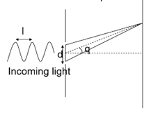
When looking at crystals, instead of using visible light we use x-rays. In this case the planes of atoms will be the d space for our split. XRD works by bouncing x-rays off of the given material where a collector then takes the diffracted beam and plots it. Because it is so fragile, in order to bounce the rays off of the material the x-ray gun is held stationary while the material and the collector arm are rotated so the results are given in 2\( \theta \).
For cubic crystals the relationship between d, our lattice parameter (a), and the miller indices (h,k,l) is given by:
Note: Miller indices are the places of atoms that scatter
Using this information, we can use the table below to determine the crystal structure:
| Bravais lattice | Constructive interference | Destructive interference |
|---|---|---|
| Reflections present | Reflections absent | |
| BCC | \( (h+k+l) \) is an even number | \( (h+k+l) \) is an odd number |
| FCC | \( h \), \( k \), \( l \) all even or all odd | \( h \), \( k \), \( l \) not all even or all odd |
XRD Excersises
Practice Problems:
- Given the information below, determine the d spacing using Bragg's law.
- Lattice parameter (a) : 0.4997 nm
- Powder x-ray : \( \lambda \)=0.1542 nm
- Using the d spacing calculated in problem 1, and the lattice parameter, a, plug in known places (111, 110, etc) to figure out what matches our given thetas, and determine the crystal structure using the table above.
Microscopy
In most materials, the constituent grains are of microscopic dimensions, having diameters that may be on the order of microns and their details must be investigated using some type of microscope. Microstructure can determine grain size and shape, and a number of other characteristics. There are a few types of microscopy we will go over today.
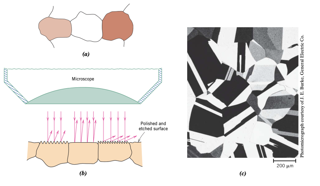
The first is called optical microscopy. With optical microscopy, a light microscope is used to study the microstructure; optical and illumination systems are its basic elements. In order to do this, we must first polish the surface of the specimen, and follow it with a surface treatment procedure called etching. Below are some illustrations that show (a) the surface structure view from a microscope, (b) the difference in how light is reflected normally to a polished and etched surface, and (c) A photomicrograph of a polycrystalline specimen showing the difference in luster and texture.
There is also something called electron microscopy, which unlike the optical microscope, this microscope uses a beam of electrons and their wave-like characteristics to magnify an object's image. This is used for things that would be too small to observe using just optical microscopy.
The last method is called scanning probe microscopy or SPM. For this method, the microscope generates a topographical map, on an atomic scale, that is a representation of surface features and characteristics of the specimen being examined.
Something that is important to look at when looking at materials is the grain size. In order to determine grain size you can either use something called linear intercept, or compare it to a standardized chart. Linear intercept is done by randomly drawing lines on a photo-micrograph depicting grain structure and then counting all the boundaries each line intercepts. First, the magnification must be determined. This is done by measuring the scale bar given and dividing it by the magnification given. For example a 15 mm scale bar that measures 100 µm would be equal to 15,000 µm ÷ 100 µm = 150× magnification. Next draw 7–10 lines and measure the total length of the lines (i.e. 6 lines at 50 mm each would total 300 mm). Finally plug all the numbers into the given equation \( \ell = \frac{L_{T}}{PM} \), where \( \ell \) is the mean intercept length, \( L_{T} \) is the total line length, \( M \) is the magnification, and \( P \) is the total number of grain boundary intersections. Relationships have been developed that relate mean intercept length to ASTM grain-size number; these are as follows:
for \( \overline{\ell} \) in mm.
for \( \overline{\ell} \) in inches.
Microscopy Excersises
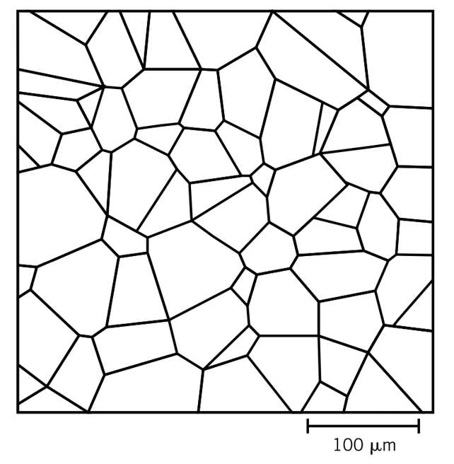
Practice Problems:The following is a schematic micrograph that represents the microstructure of some hypothetical metal. Determine the following:
- Mean Intercept length
- ASTM grain-size number, G